28
9151AINDCO07/09
ATA8742
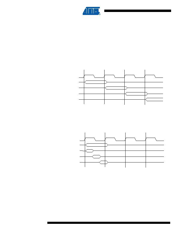
12.7 Instruction Execution Timing
This section describes the general access timing concepts for instruction execution. The AVR
CPU is driven by the CPU clock clk
CPU
, directly generated from the selected clock source for the
chip. No internal clock division is used.
Figure 12-4 on page 28 shows the parallel instruction fetches and instruction executions
enabled by the Harvard architecture and the fast access Register File concept. This is the basic
pipelining concept to obtain up to 1 MIPS per MHz with the corresponding unique results for
functions per cost, functions per clocks, and functions per power-unit.
Figure 12-4. The Parallel Instruction Fetches and Instruction Executions
Figure 12-5 on page 28 shows the internal timing concept for the Register File. In a single clock
cycle an ALU operation using two register operands is executed, and the result is stored back to
the destination register.
Figure 12-5. Single Cycle ALU Operation
12.8 Reset and Interrupt Handling
The AVR provides several different interrupt sources. These interrupts and the separate Reset
Vector each have a separate Program Vector in the Program memory space. All interrupts are
assigned individual enable bits which must be written logic one together with the Global Interrupt
Enable bit in the Status Register in order to enable the interrupt.
The lowest addresses in the Program memory space are by default defined as the Reset and
Interrupt Vectors. The complete list of vectors is shown in
Interrupts
on page 66. The list also
determines the priority levels of the different interrupts. The lower the address the higher is the
priority level. RESET has the highest priority, and next is INT0 the External Interrupt Request
0.
clk
1st Instruction Fetch
1st Instruction Execute
2nd Instruction Fetch
nd Instruction Execute
3rd Instruction Fetch
rd Instruction Execute
4th Instruction Fetch
T1
T2
T3
T4
CPU
Total Execution Time
egister Operands Fetch
ALU Operation Execute
Result Write Back
T1
T2
T3
T4
clk
CPU
发布紧急采购,3分钟左右您将得到回复。
相关PDF资料
ATA8743-PXQW
MCU W/TRANSMITTER ASK/FSK 24QFN
ATAVRRZ200
KIT DEMO AT86RF230
AV101-12LF
ATTENUATOR HIP3 0.70-1GHZ 8-SOIC
AV102-12LF
ATTENUATOR HIP3 1.7-2GHZ 8SOIC
AV113-12LF
ATTENUATOR HIP3 2.1-2.3GHZ 8SOIC
AXUV100G
SENSOR ELECTRON DETECTION
B0205F50200AHF
XFRMR BALUN RF 200-500MHZ 1608
B0310J50100AHF
XFRMR BALUN RF 300-1000MHZ 0805
相关代理商/技术参数
ATA8743
制造商:ATMEL 制造商全称:ATMEL Corporation 功能描述:Microcontroller with UHF ASK/FSK Transmitter
ATA8743C- PXQW
功能描述:8位微控制器 -MCU Embedded uC incl RF Tx for 315 MHz
RoHS:否 制造商:Silicon Labs 核心:8051 处理器系列:C8051F39x 数据总线宽度:8 bit 最大时钟频率:50 MHz 程序存储器大小:16 KB 数据 RAM 大小:1 KB 片上 ADC:Yes 工作电源电压:1.8 V to 3.6 V 工作温度范围:- 40 C to + 105 C 封装 / 箱体:QFN-20 安装风格:SMD/SMT
ATA8743C-PXQW
制造商:Atmel Corporation 功能描述:EMBEDDED ?C INCL RF TX FOR 868 MHZ - Trays 制造商:Atmel Corporation 功能描述:EMBEDDED C INCL 868MHZ TX
ATA8743C-PXQW-1
功能描述:EMBEDDED INCL RF TX FOR 868 MHZ 制造商:microchip technology 系列:- 包装:剪切带(CT) 零件状态:在售 频率:868MHz ~ 928MHz 应用:通用 调制或协议:UHF 数据速率(最大值):32kbps 功率 - 输出:5.5dBm 电流 - 传输:9.8mA 数据接口:SPI 天线连接器:PCB,表面贴装 存储容量:4kB 闪存,256B EEPROM,256B SRAM 特性:- 电压 - 电源:2 V ~ 4 V 工作温度:-40°C ~ 85°C 封装/外壳:24-VQFN 裸露焊盘 标准包装:1
ATA8743-PXQW
功能描述:8位微控制器 -MCU Embedded uC incl RF Tx for 315 MHz
RoHS:否 制造商:Silicon Labs 核心:8051 处理器系列:C8051F39x 数据总线宽度:8 bit 最大时钟频率:50 MHz 程序存储器大小:16 KB 数据 RAM 大小:1 KB 片上 ADC:Yes 工作电源电压:1.8 V to 3.6 V 工作温度范围:- 40 C to + 105 C 封装 / 箱体:QFN-20 安装风格:SMD/SMT
ATAB5275
功能描述:射频开发工具 LF Tx Antenna driver board (TPMS) RoHS:否 制造商:Taiyo Yuden 产品:Wireless Modules 类型:Wireless Audio 工具用于评估:WYSAAVDX7 频率: 工作电源电压:3.4 V to 5.5 V
ATAB5276
功能描述:射频开发工具 1A Antenna Driver Demoboard RoHS:否 制造商:Taiyo Yuden 产品:Wireless Modules 类型:Wireless Audio 工具用于评估:WYSAAVDX7 频率: 工作电源电压:3.4 V to 5.5 V
ATAB5278
功能描述:射频开发工具 LF Tx Antenna driver board (PEG) RoHS:否 制造商:Taiyo Yuden 产品:Wireless Modules 类型:Wireless Audio 工具用于评估:WYSAAVDX7 频率: 工作电源电压:3.4 V to 5.5 V